
Security News
Deno 2.6 + Socket: Supply Chain Defense In Your CLI
Deno 2.6 introduces deno audit with a new --socket flag that plugs directly into Socket to bring supply chain security checks into the Deno CLI.
By Sarah Gooding - Dec 12, 2025
gds2palace
Advanced tools
gds2palace provides utility functions for an RFIC FEM simulation workflow based on the Palace FEM solver by AWS.
The full repository with examples is available at https://github.com/VolkerMuehlhaus/gds2palace_ihp_sg13g2
Extensive documentation on creating models using gds2palace is available in PDF format here: gds2palace FEM workflow for IHP
To install the gds2palace module, activate the venv where you want to install.
Documentation for the gds2palace workflow assumes that you have created a Python venv named "palace" in ~/venv/palace and installed the modules there.
If you follow this, you would first activate the venv:
source ~\venv\palace\bin\activate
and then install gds2palace module and dependencies via PyPI:
pip install gds2palace
To upgrade to the latest version, do
pip install gds2palace --upgrade
This module also installs these dependencies: gdspy > 1.6.0 gmsh PySide6
PySide6 is not required by gds2palace module itself, but required by the GUI application that uses gds2palace.
Below is an example script that create *.json and *msh input files for simulation with Palace. Input is a layout in GDSII file format and an XML file with stackup information
import os
import sys
import subprocess

from gds2palace import *

# ===================== input files and path settings =======================

gds_filename = "line_simple_viaport.gds"   # geometries
XML_filename = "SG13G2_nosub.xml"          # stackup

# preprocess GDSII for safe handling of cutouts/holes?
preprocess_gds = False

# merge via polygons with distance less than .. microns, set to 0 to disable via merging.
merge_polygon_size = 0

# get path for this simulation file
script_path = utilities.get_script_path(__file__)

# use script filename as model basename
model_basename = utilities.get_basename(__file__)

# set and create directory for simulation output
sim_path = utilities.create_sim_path (script_path,model_basename)
print('Simulation data directory: ', sim_path)

# change path to models script path
modelDir = os.path.dirname(os.path.abspath(__file__))
os.chdir(modelDir)

# ======================== simulation settings ================================

settings = {}

settings['unit']   = 1e-6  # geometry is in microns
settings['margin'] = 50    # distance in microns from GDSII geometry boundary to simulation boundary

settings['fstart']  = 0e9
settings['fstop']   = 100e9
settings['fstep']   = 2.5e9

settings['refined_cellsize'] = 2  # mesh cell size in conductor region
settings['cells_per_wavelength'] = 10   # how many mesh cells per wavelength, must be 10 or more

settings['meshsize_max'] = 70  # microns, override cells_per_wavelength
settings['adaptive_mesh_iterations'] = 0

# settings['nogui'] = True  # create files without showing 3D model
# settings['nogui'] = ('nogui' in sys.argv)  # check if nogui specified on command line, then create files without showing 3D model

# Ports from GDSII Data, polygon geometry from specified special layer
# Excitations can be switched off by voltage=0, those S-parameter will be incomplete then

simulation_ports = simulation_setup.all_simulation_ports()
# instead of in-plane port specified with target_layername, we here use via port specified with from_layername and to_layername
simulation_ports.add_port(simulation_setup.simulation_port(portnumber=1, voltage=1, port_Z0=50, source_layernum=201, from_layername='Metal1', to_layername='TopMetal2', direction='z'))
simulation_ports.add_port(simulation_setup.simulation_port(portnumber=2, voltage=1, port_Z0=50, source_layernum=202, from_layername='Metal1', to_layername='TopMetal2', direction='z'))


# ======================== simulation ================================

# get technology stackup data
materials_list, dielectrics_list, metals_list = stackup_reader.read_substrate (XML_filename)
# get list of layers from technology
layernumbers = metals_list.getlayernumbers()
layernumbers.extend(simulation_ports.portlayers)

# read geometries from GDSII, only purpose 0
allpolygons = gds_reader.read_gds(gds_filename, layernumbers, purposelist=[0], metals_list=metals_list, preprocess=preprocess_gds, merge_polygon_size=merge_polygon_size)


########### create model ###########

settings['simulation_ports'] = simulation_ports
settings['materials_list'] = materials_list
settings['dielectrics_list'] = dielectrics_list
settings['metals_list'] = metals_list
settings['layernumbers'] = layernumbers
settings['allpolygons'] = allpolygons
settings['sim_path'] = sim_path
settings['model_basename'] = model_basename


# list of ports that are excited (set voltage to zero in port excitation to skip an excitation!)
excite_ports = simulation_ports.all_active_excitations()
config_name, data_dir = simulation_setup.create_palace (excite_ports, settings)
XML file for this example:
<Stackup schemaVersion="2.0">
<Materials>
<Material Name="Activ" Type="Conductor" Permittivity="1" DielectricLossTangent="0" Conductivity="357141.0" Color="00ff00"/>
<Material Name="Metal1" Type="Conductor" Permittivity="1" DielectricLossTangent="0" Conductivity="21640000.0" Color="39bfff"/>
<Material Name="Metal2" Type="Conductor" Permittivity="1" DielectricLossTangent="0" Conductivity="23190000.0" Color="ccccd9"/>
<Material Name="Metal3" Type="Conductor" Permittivity="1" DielectricLossTangent="0" Conductivity="23190000.0" Color="d80000"/>
<Material Name="Metal4" Type="Conductor" Permittivity="1" DielectricLossTangent="0" Conductivity="23190000.0" Color="93e837"/>
<Material Name="Metal5" Type="Conductor" Permittivity="1" DielectricLossTangent="0" Conductivity="23190000.0" Color="dcd146"/>
<Material Name="TopMetal1" Type="Conductor" Permittivity="1" DielectricLossTangent="0" Conductivity="27800000.0" Color="ffe6bf"/>
<Material Name="TopMetal2" Type="Conductor" Permittivity="1" DielectricLossTangent="0" Conductivity="30300000.0" Color="ff8000"/>
<Material Name="TopVia2" Type="Conductor" Permittivity="1" DielectricLossTangent="0" Conductivity="3143000.0" Color="ff8000"/>
<Material Name="TopVia1" Type="Conductor" Permittivity="1" DielectricLossTangent="0" Conductivity="2191000.0" Color="ffe6bf"/>
<Material Name="Via4" Type="Conductor" Permittivity="1" DielectricLossTangent="0" Conductivity="1660000.0" Color="deac5e"/>
<Material Name="Via3" Type="Conductor" Permittivity="1" DielectricLossTangent="0" Conductivity="1660000.0" Color="9ba940"/>
<Material Name="Via2" Type="Conductor" Permittivity="1" DielectricLossTangent="0" Conductivity="1660000.0" Color="ff3736"/>
<Material Name="Via1" Type="Conductor" Permittivity="1" DielectricLossTangent="0" Conductivity="1660000.0" Color="ccccff"/>
<Material Name="Cont" Type="Conductor" Permittivity="1" DielectricLossTangent="0" Conductivity="2390000.0" Color="00ffff"/>
<Material Name="Passive" Type="Dielectric" Permittivity="6.6" DielectricLossTangent="0.0" Conductivity="0" Color="a0a0f0"/>
<Material Name="SiO2" Type="Dielectric" Permittivity="4.1" DielectricLossTangent="0.0" Conductivity="0" Color="fffcad"/>
<Material Name="Substrate" Type="Semiconductor" Permittivity="11.9" DielectricLossTangent="0" Conductivity="2.0" Color="01e0ff"/>
<Material Name="EPI" Type="Semiconductor" Permittivity="11.9" DielectricLossTangent="0" Conductivity="5.0" Color="294fff"/>
<Material Name="AIR" Type="Dielectric" Permittivity="1.0" DielectricLossTangent="0.0" Conductivity="0" Color="d0d0d0"/>
<Material Name="LOWLOSS" Type="Conductor" Permittivity="1" DielectricLossTangent="0" Conductivity="1E10" Color="ff0000"/>
<Material Name="Vmim" Type="Conductor" Permittivity="1" DielectricLossTangent="0" Conductivity="2191000.0" Color="ffe6bf"/>
<Material Name="MIM" Type="Conductor" Permittivity="1" DielectricLossTangent="0" Conductivity="500000.0" Color="e6ffbf"/>
</Materials>
<ELayers LengthUnit="um">
<Dielectrics>
<Dielectric Name="AIR" Material="AIR" Thickness="300.0000"/>
<Dielectric Name="Passive" Material="Passive" Thickness="0.4000"/>
<Dielectric Name="SiO2" Material="SiO2" Thickness="15.7303"/>
<Dielectric Name="Spacing" Material="SiO2" Thickness="2.0"/>
</Dielectrics>
<Layers>
<Substrate Offset="2.0"/>
<Layer Name="Activ" Type="conductor" Zmin="0.0000" Zmax="0.4000" Material="Activ" Layer="1"/>
<Layer Name="Metal1" Type="conductor" Zmin="1.0400" Zmax="1.4600" Material="Metal1" Layer="8"/>
<Layer Name="Metal2" Type="conductor" Zmin="2.0000" Zmax="2.4900" Material="Metal2" Layer="10"/>
<Layer Name="Metal3" Type="conductor" Zmin="3.0300" Zmax="3.5200" Material="Metal3" Layer="30"/>
<Layer Name="Metal4" Type="conductor" Zmin="4.0600" Zmax="4.5500" Material="Metal4" Layer="50"/>
<Layer Name="Metal5" Type="conductor" Zmin="5.0900" Zmax="5.5800" Material="Metal5" Layer="67"/>
<Layer Name="TopMetal1" Type="conductor" Zmin="6.4303" Zmax="8.4303" Material="TopMetal1" Layer="126"/>
<Layer Name="TopMetal2" Type="conductor" Zmin="11.2303" Zmax="14.2303" Material="TopMetal2" Layer="134"/>
<Layer Name="TopVia2" Type="via" Zmin="8.4303" Zmax="11.2303" Material="TopVia2" Layer="133"/>
<Layer Name="TopVia1" Type="via" Zmin="5.5800" Zmax="6.4303" Material="TopVia1" Layer="125"/>
<Layer Name="Via4" Type="via" Zmin="4.5500" Zmax="5.0900" Material="Via4" Layer="66"/>
<Layer Name="Via3" Type="via" Zmin="3.5200" Zmax="4.0600" Material="Via3" Layer="49"/>
<Layer Name="Via2" Type="via" Zmin="2.4900" Zmax="3.0300" Material="Via2" Layer="29"/>
<Layer Name="Via1" Type="via" Zmin="1.4600" Zmax="2.0000" Material="Via1" Layer="19"/>
<Layer Name="Cont" Type="via" Zmin="0.4000" Zmax="1.0400" Material="Cont" Layer="6"/>
<Layer Name="MIM" Type="conductor" Zmin="5.6043" Zmax="5.7540" Material="MIM" Layer="36"/>
<Layer Name="Vmim" Type="via" Zmin="5.7540" Zmax="6.4303" Material="Vmim" Layer="129"/>
</Layers>
</ELayers>
</Stackup>
FAQs
Create AWS Palace model from RFIC GDSII layout file
We found that gds2palace demonstrated a healthy version release cadence and project activity because the last version was released less than a year ago. It has 1 open source maintainer collaborating on the project.
Did you know?

Socket for GitHub automatically highlights issues in each pull request and monitors the health of all your open source dependencies. Discover the contents of your packages and block harmful activity before you install or update your dependencies.
Security News
Deno 2.6 introduces deno audit with a new --socket flag that plugs directly into Socket to bring supply chain security checks into the Deno CLI.
Security News
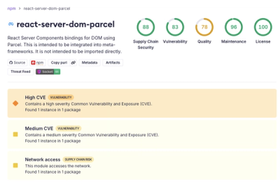
New DoS and source code exposure bugs in React Server Components and Next.js: what’s affected and how to update safely.

Security News
Socket CEO Feross Aboukhadijeh joins Software Engineering Daily to discuss modern software supply chain attacks and rising AI-driven security risks.